The physical design process is crucial in transforming chip designs into real-world products that drive our digital world. It involves a carefully planned series of steps aimed at optimizing chip layouts for performance, power efficiency, and manufacturability. But what are these steps, and how do they fit into the broader design process? Let’s dive into the complexities of physical design and explore its key stages.
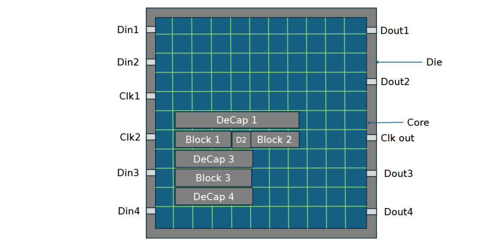
First we define the size of Core and Die. The netlist sits in the core area, surrounding the core area is the die section. The we define the pre-placed cells which are based on pre-defined functions having some combinational logic, the goal is to put the pre-placed cells in optimal area for close access to its input/output pins. We surround the pre-placed cells with decoupling capacitors, the reason we do that is because there is a current requirement in the cells in pre-placed blocks, and drawing high current on demand will need some capacitors to avoid large slew. The power supply on the chip is also optimized to be distributed in a grid manner, the Vdd and Vss grid lines are present in the core, so power can be pulled from the closest point to help reduce slew during signal changes.
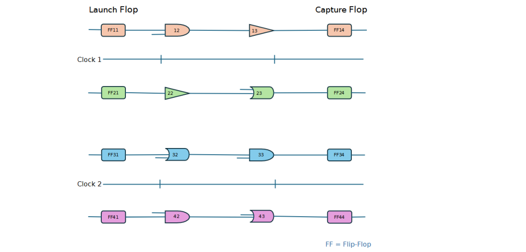
Lets say we have to place the above netlist on the core.
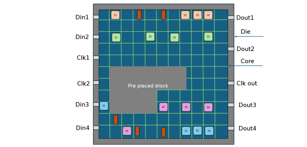
We have to consider that all the wires connecting the various gates will have some capacitance and resistance. So it the wire length is long then we will want to put some buffers in between. The combinational delay of a route is a sum of delays introduced by each element and the connecting wires between them. For a given route this has to be less than a certain value defined by clock to function properly.
Noise Margin, Decoupling Capacitors

For any signal to be considered as 0 or 1, it has to be in NM (NMl or NMh) areas, In undefined region the signal value can go in either direction, If there is a bump in supply voltage which goes up to only to the undefined area because of long wire lengths, we will not get desired results. So to avoid that a de-coupling capacitor is used which will store the charge and ensure the voltage level is reached to put the signal in range to be considered as 0 or 1. The other way to manage the immediate need for a huge power supply will be to decentralize the power supply and let the circuit draw power from the nearest section of the power grid.
Voltage Droop or Ground bump
When there is a switch of multiple gates on the same power line and the result needs to draw more power, then the input power experiences a slight drop called Voltage droop. Similarly if lot of gates switch to 0 simultaneously on a line, then they all discharge their voltage into the same ground line causing a Ground bump. This may cause the result to go into the undefined category then the result becomes unpredictable.
Timing Analysis (Ideal clock)
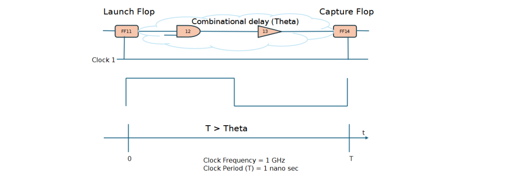
Lets assume the clock is having a frequency of 1 Ghz, so the clock wave period is 1 nano second. The edge of the clock wave reaches from launch flop to capture flop in 1 nano second for one wave, so for this circuit to work, the work by the circuit has to be completed within one clock cycle, so the combinational delay (Theta) between the launch and capture flops should be less than the clock time period (T).
The combinational delay of a path (lets say the first circuit) is defined as
Theta = FlipFlop 11 delay
      + Wire FF11 - Buf1 estimated delay
      + Buf1 delay
      + Wire Buf1 - Buf2 estimated delay
      + Buf2 delay
      + Wire Buf2 - 12 estimated delay
      + delay of logic cell 12
      + Wire 12 - 13 estimated delay
      + delay of logic cell 13
      + Wire 13 - FF14 estimated delay
Note: FlipFlop 14 delay is Not included since we are calculating delay of the circuit between FF1 and FF2
D Flip-flop

A flip-flop has multiple Mosfets, logic gates and wiring which has its own resistance and capacitance. The way the flipflop works is It allows the reading of the input (D) only at the rising/positive edge of the clock https://www.electronicsforu.com/technology-trends/learn-electronics/flip-flop-rs-jk-t-d . On the edge of the clock the input reaches the first logic gate, and then the output takes some finite time to reach to the next gates. This is called a setup delay time, for the input to settle midway to D flop. So we add the setup time to the combinational delay and this value now has to be less than the clock time.
Adding Clock jitter

The clock will not be able to provide an edge at 0 or T seconds. That is because it has its own inbuilt variation because the clock source is based off on some real circuitry which has its own delays. So the Clock time should be more than the combinational delay added because of clock jitter too.
Introducing multiple clocks
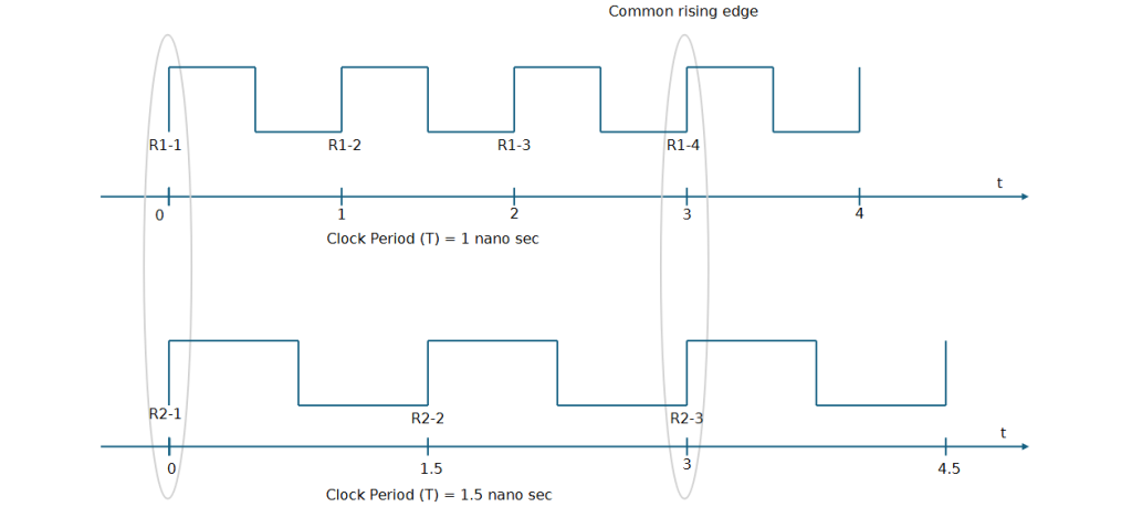
Lets say we have 2 clocks, Clock 1 has a time period of 1 nano second, and Clock 2 has a time period of 1.5 nano seconds. Lets assume the Clock 1 is connected to Launch flop and Clock 2 is connected to capture flop. So in the above diagram, we see that at time 0 we have a common rising edge in both clocks. This common rising edge occurs after next 3 nano seconds. What we need is the minimum duration between 2 rising edges.
We calculate the difference in rising edges from launch clock to Capture flop clock
R2-2 - R1-1 = 1.5 nano second
R2-2 - R1-2 = 0.5 nano second
R2-3 - R1-3 = 1.0 nano second
So our window gets reduced to 0.5 nano seconds since data can be launched at R1-2 (1 ns) and needed to be captured at R2-2 (1.5 ns) which is just a difference of 0.5 nano second. This is called shortest window (SW).
We had
T > Theta + S + U
Where T was the clock time. So we need to replace it with Shortest window, making the equation
SW > Theta + S + U
Rearranging for Theta
SW - S - U > Theta
Shortest window - setup delay - clock uncertainty > combinational delay
Data Slew

When the signal goes from 0 to 1, or from 1 to 0, there is some time needed to make the transition. The circuits at each states, the logic gates all require this slew to be within a specified range to work properly.
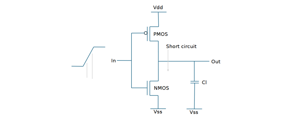
When a slew occurs from 0 to 1, the PMOS is supposed to be switched from ON to OFF and NMOS transistion from OFF to ON. There is a range of current in slew where the PMOS is getting turned OFF and NMOS is getting turned ON. During that time both are in ON state, so there is a shortcircuit from supply to ground during that time. And if the slew is longer, the more power dissipation happens during the short circuit.
To reduce the shortcircuit, we put a load capacitor at the end, if this capacitance is very high, then the short circuit current to ground will be less, but the output waveform slew will be longer since it will take more time to charge/discharge the capacitor and it will be impact the downstream circuit, but if the capacitance is very low, then short circuit current to ground will be large and output slew will be small. We need to optimize the output load capacitor to manage the slew of the output waveform.
Clock tree

We have a clock port which has to reach some flip-flops. When we do the wiring, we have to ensure that the time which is required by clock to reach the first flip flop is t1, and for the second flip flop its t2. These are different because of physical distance differences. The time difference is called Skew which is calculated as t2 – t1. Our goal is to have it as close to 0 as possible.

To Solve this we use a mid point strategy, we find the mid point to the flip flops, and then again find a second midpoint, forming a tree of connections to ensure the physical distance from clock port is same for all flip flops. This ensures the skew to be very close to 0.
Cheers!! – Amit Tomar


