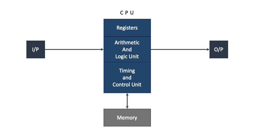
There are 3 core parts inside a CPU.
– Registers – Used to store data during processing
– Arithmetic and Logical Unit – Performs arithmetic operations like addition, multiplication, division and the Logical unit performs operations like AND, OR, XOR, NOT
– Timing and Control Unit – generates signals required for proper operation of CPU.
The CPU communicates with memory to read and write data, It also sends output to devices like printer, monitor. The Input device like keyboard, mouse is used to send data to CPU to perform operations based on program stored in memory.

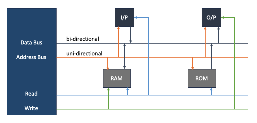
A BUS is a group of wires on which same type of signal flows.
There are 2 main types of data bus in microprocessor which communicate with I/P, O/P and memory devices.
The data bus is bi-directional and is responsible to bring data to and from various components of computer.
The address bus is uni-directional and is responsible to denote address of the the modules and storage.
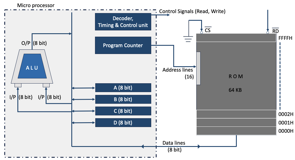
The Timing and Control unit generates Read and Write signals along with other signals. When the processor want to read the data, it generates a read signal, along with the address on the address bus from where it wants to read the data. The data then flows to the CPU using the data bus.

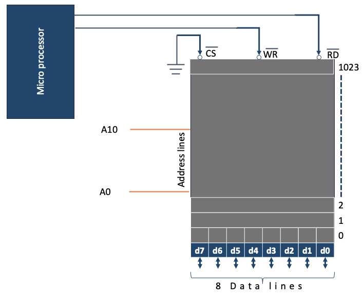
The memory has addressed locations where data is stored. Each location can store 8 bits, 16 bits, 32 bits of data which is defined by the number of data lines in the data bus. In one clock cycle the data at 1 location is moved to or read from memory location using the data lines.
The size of the memory is defined by the number of address lines. So if there are 10 address lines, the maximum number of addressed which can be assigned are 2^10 which is 1024 (1 KB) and to have 64 KB (2^16) memory we will need 16 address lines and so on.
The Chip Select CS pin is used to select the memory, whenever the microprocessor wants to communicate with the memory, it will use the CS pin to mark the memory as selected.
There are 2 more pins Read and Write which are marked by processor when it wants to read or write to this memory. All these pins are active low pins, which means a zero indicates an activated pin.

The memory like RAM/ROM sits outside the processor, the registers are part of processor and special name is given by the manufacturer to the registers which is used to access the register like A, B, C, D. and these registers can have 8bit capacity or 16 bit and so on.
There is a decoder in processor which translates the instruction which is sent to processor telling it what to perform, and timing and control unit will generate appropriate signals to work on the instruction.
There is a 16 bit register in 8051 which is called Program Counter which stores the next memory location from where processor is going to fetch the next instruction.
The 8 bit data lines signify the amount of data the processor sends or receives in 1 clock cycle, so a 8 bit processor will send or receive 8 bits at a time.
To send instruction to the processor we have to write a program which can be understood by the processor.
Machine language also called low level language is written in binary format, The binary instruction to operation information is already integrated / stored in the decoder, and has to be used while writing the program. All instructions in this machine language program are written in binary format.
Binary pattern 1 : Add content of register A & B and put result in register A
Binary pattern 2 : Add content of register B & C and put result in register B
Binary pattern 3 : Add content of register C & a given number and put result in register C
These patterns are hardware dependent and cannot be used on any other processor.
Assembly language uses mnemonics which are english like words which represent operation or instruction.
Add A, B : Binary pattern 1 : Add content of register A & B and put result in register A
Add B, C : Binary pattern 2 : Add content of register B & C and put result in register B
Add C, #20H: Binary pattern 3 : Add content of register C & a given number which is next in memory and put result in register C
The decoder helps translate the mnemonic to instruction for the processor. This is also hardware dependent since different hardware will have different registers, sizes and capabilities.
High level language like C, C++ use compiler to translate the code to the particular processor.

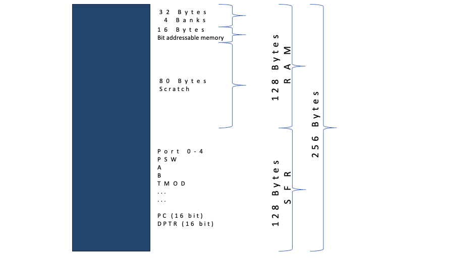
The 8051 microcontoller has 128 Bytes of RAM. It uses 8 bits to define memory address, and defines 2^8 (256) addresses
The remaining 128 addresses are used to define the location of Special function registers

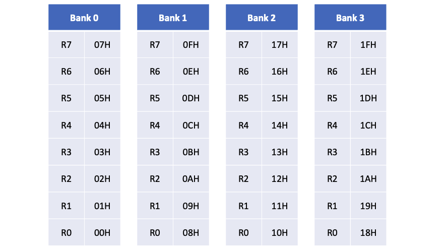
The first 32 bytes in RAM are used by the 4 banks, each bank is 8 Byte and and its label is in range of R0 to R7. The Banks uses the address range from 00H to 1FH
The instruction can use the label R0, R1 etc, or the memory address in the instruction, but since all four banks have same label, we need to use the 2 bits in PSW register to indicate which Bank is active

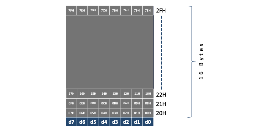
Bit addressable memory spans 16 bytes from 20H to 2FH. Each bit is addressable so its addressed which can be recognized by processor. The bits addresses range from 00H to 7FH
Since the addresses overlap with the range in memory (0BH is Bank 1, R3 and is also the fourth bit in 21H location) the instruction guides whether the data has to be referred to the Byte or the bit
Mov A, 0BH will move the Byte from Bank 1, R3 into A register
Mov C, 0BH will move the bit from fourth bit in 21H location) into carry flag location in PSW.

The Program Status Word is a 8 bit Special Function Register located at D0H. It contains 4 conditional flags to denote the status of the registers
Bit 7 – Carry Flag is set during unsigned arithmetic operation from the MSB (most significant bit). If in addition we get a carry, or in subtraction we need a borrow from MSB then this flag will be set to 1.
Bit 6 – Auxiliary Carry Flag is a non programmable flag (cannot read/write this directly, used only by processor indirectly) is used to convert Decimal number to BCD (Binary Coded Decimal number). When a carry/borrow is generated from 4th bit (MSB of lower nibble) then this flag is set to 1.
Bit 5 is unused
Bit 4 & 3 are used to select the Banks, 00 will mean Bank 0, 01 is Bank 1, 10 is Bank 2, 11 is Bank 3
Bit 2 – Overflow flag is set during signed arithmetic operation
Bit 1 is not used
Bit 0 is the Parity bit which is set to 1 if after a operation the number of Ones are odd.
If we want to access a single bit from PSW, then we can use PSW.0 PSW.2 etc. since PSW is bit addressable.


Next time I will cover some details on assembly language.
Cheers – Amit Tomar

