Today we will learn about some hardware concepts, how ASIC (Application specific Integrated circuit) chips are designed in verilog and some history behind it.
HDL – Hardware description Language
In computer engineering, a HDL serves as a specialized computerized means of delineating the arrangement and functionality of electronic circuits, predominantly those of a digital logic nature.
The utilization of a hardware description language facilitates the creation of an accurate and systematic portrayal of an electronic circuit, allowing for automated analysis and simulation thereof. Additionally, it enables the synthesis of the HDL description into a netlist—an explicit specification detailing the physical electronic components and their interconnections. Subsequently, this netlist can be arranged and routed to generate the requisite set of masks essential for the fabrication of an integrated circuit.
A hardware description language bears a resemblance to programming languages like C or ALGOL, adopting a textual format that encompasses expressions, statements, and control structures. However, a notable distinction between most programming languages and HDLs lies in the explicit inclusion of temporal considerations within the latter.
HDLs are an integral component of electronic design automation (EDA) systems, particularly for intricate circuits such as application-specific integrated circuits, microprocessors, and programmable logic devices.
PLD – Programmable Logic Device
A PLD is an electronic entity employed in the creation of adaptable digital circuits. Unlike discrete logic gates, which possess fixed functionalities, a PLD lacks a predetermined function upon manufacturing. Prior to its incorporation within a circuit, the PLD necessitates programming to embody the intended functionality. In contrast to fixed logic devices, programmable logic devices streamline the design process for intricate logic systems and may provide enhanced performance capabilities. Notably, programming a PLD entails modifying the interconnections established between the internal gates of the device, distinguishing it from the programming process employed for microprocessors. It can be categorized further as PLA, PAL, CLPD or FPGA
PLA – Programmable logic array
A PLA consist of 2 planes which contain interconnected AND and OR gates with input buffers and inverters. The first plane contains AND gates and the second plan uses the output of first plane as inputs and contains programmable OR gates. To configure it to a desired implementation, the design it etched into it by burning off some of the gate switches which are made of nichrome wire which vaporizes on passing high voltage in it.
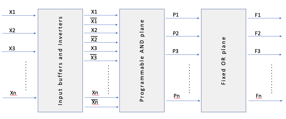
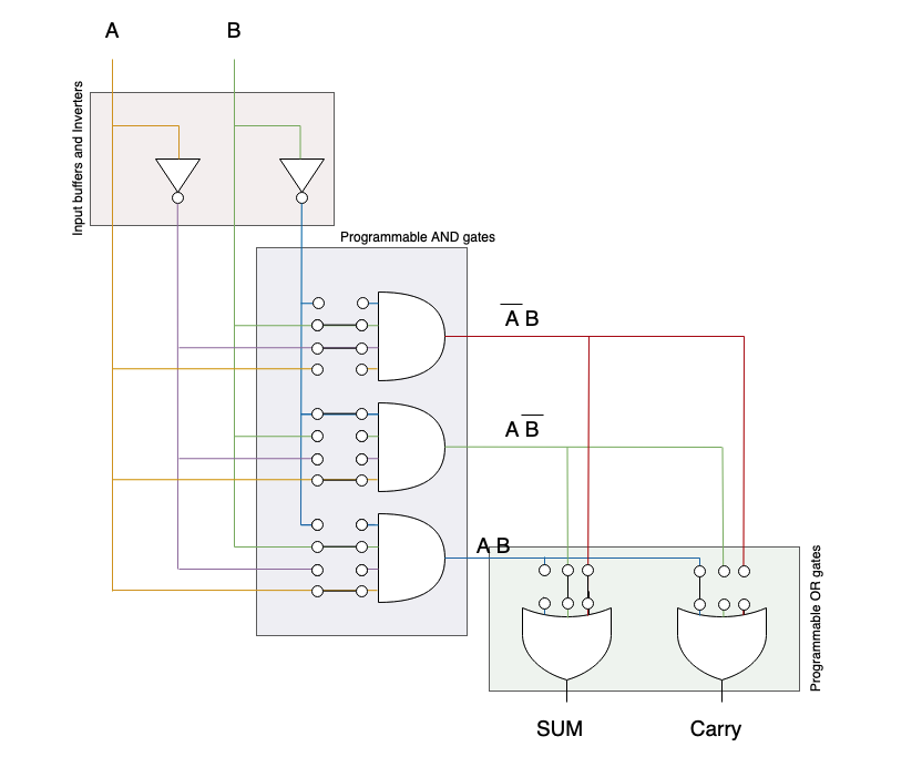
The planes have interconnected gates with switches as below and the unwanted connections are burnt off based on the design. Below is an example of 2 input 2 output PLA.
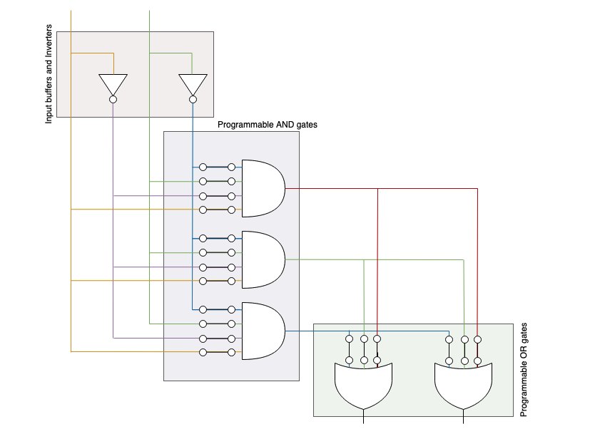
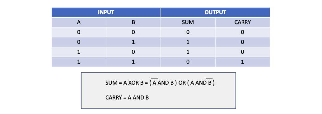
Lets assume we want to create a half adder which sums up 2 input bits and outputs the sum and a carry.

This is the truth table and formula for half adder
We have a PLA which is connected like above and we have to make it into this structure
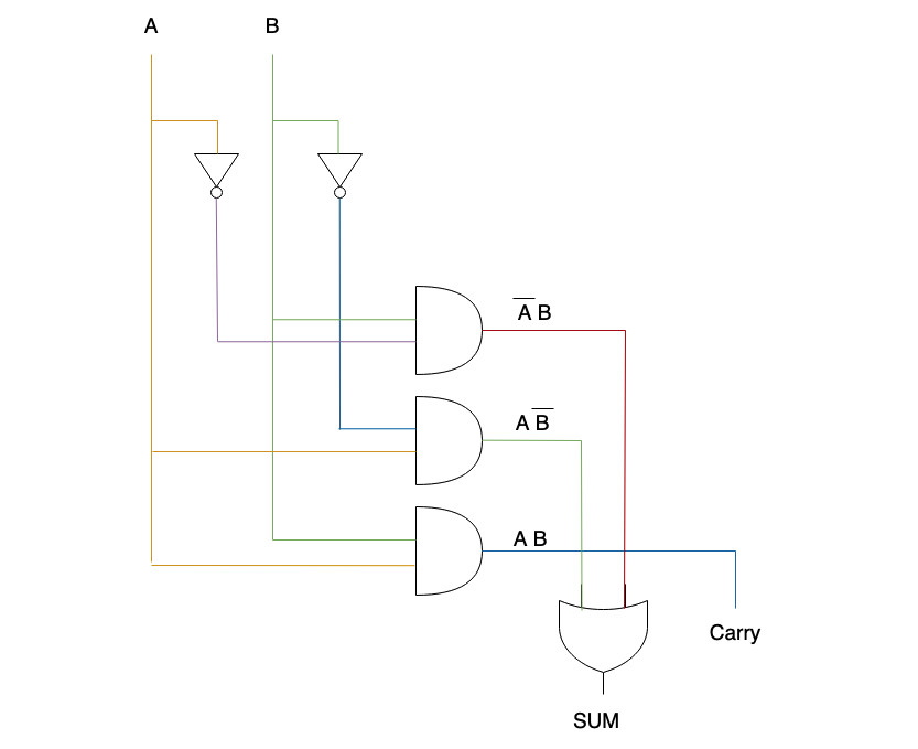
After we load our design on the PLA, the resultant PLA will look like
PAL – Programmable Array Logic
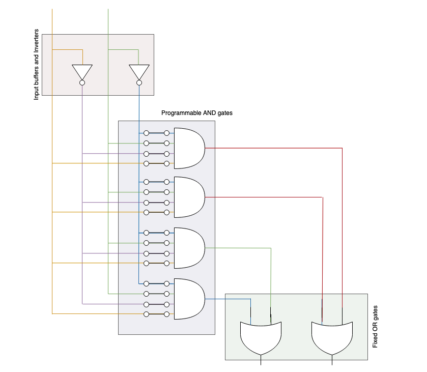
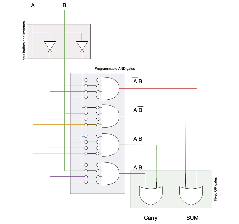
Just like PLA, the PAL has 2 planes, the first one being a programmable AND plan to generate product. This output will be sent through the FIXED OR plane.
The switches which are configurable in PLDs introduce a delay, to avoid this delay, the OR plane in PAL is hard-wired which increases performance but reduces flexibility.

This is a example of a 2 input 2 output PAL
If we want to implement the same half adder as above in PAL, then it will look like
CPLD – Complex Programmable Logic Device
CPLD is very similar to a PAL, but it has many planes, which is why its more complex and called Complex PLD
FPGA – Field-programmable gate array
FPGAs contain an array of programmable logic blocks, and a hierarchy of reconfigurable interconnects allowing blocks to be wired together.
Instead of burning off the switches, the FPGA is a programmable module, which can be reused and made the PLDs obsolete.
Xilinx produced the first commercially viable field-programmable gate array in 1985
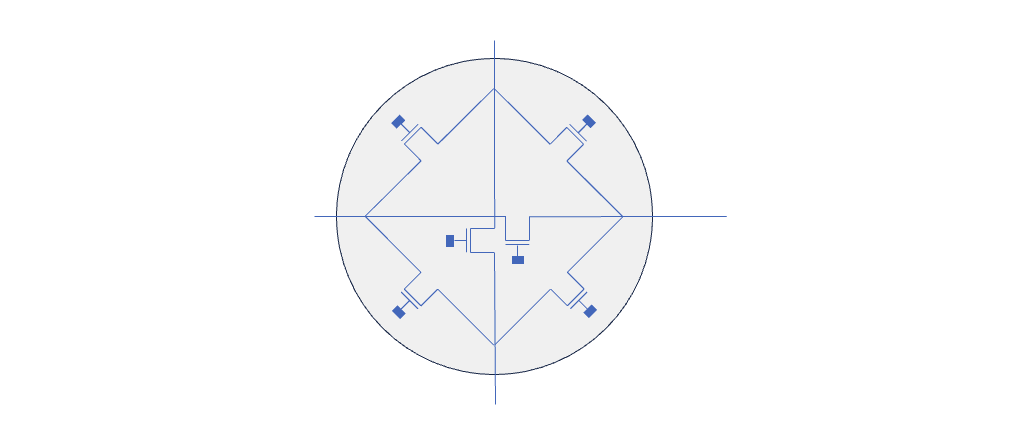
A FPGA module looks like a matrix of interconnected modules which route the electricity to right configurable logic block
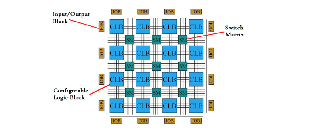
There are 2 core components in FPGA
PSM – Programmable switch module are made up of 6 mosfets to route the electric current to the right output wire. Which mosfet is ON/OFF is stored in in 1 bit SRAM cell associated with each nmos
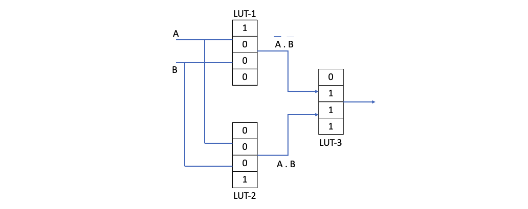
CLB – Configurable logic Blocks are configured using LUTs – Lookup tables, which is simply a map of input to output. It just maintains a desired mapping of all possible inputs and when it receives an input, it looks it up in that table and returns the corresponding output. We can say it just stores the truth tables
When we write out HDL program, we do not know which CLB will be containing which logic portion. When we do the synthesis, the input to it will be which FPGA model is used in synthesis, there the tool will divide the logic onto LUTs, but still it won’t define which specific CLB will be containing which LUT.
When we pass the EDIF file through Place and Route tool, then only CLB to LUT mapping will be generated.
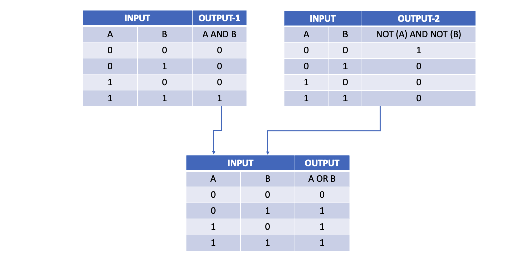
Lets say we are writing a logic for
F = (X AND Y) OR (NOT(X) AND NOT(Y))
3 truth tables which will be created for this design are
These 3 truth tables will get deployed as LUTs on the CLBs like
Modelling Level
In Verilog VHDL we can define the design using multiple approaches. We can specify how each mosfet is connected to the others, or we can just explain what our results will be and let the synthesizer come up with the combination which is best fit for us
A full adder takes in 2 bits to be added, and a carry which is coming in from previous adder. The output is the sum of the bits, and a carry.

If we want to build a 3 bit adder, we have to interconnect 3 adders in series
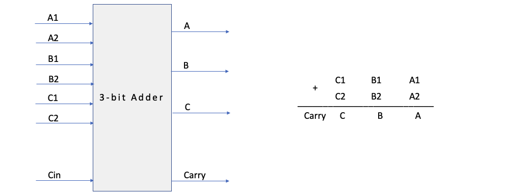
And this is a representation of how a 3 bit adder is implemented using 3 full adders

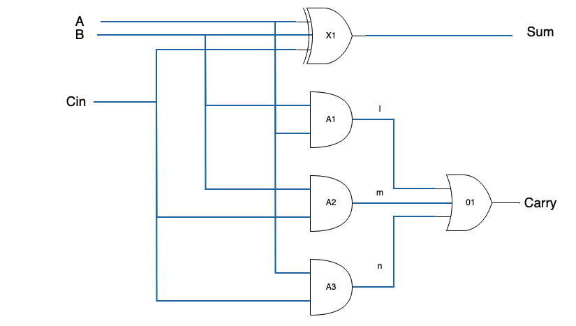
This is the implementation of a full adder
This is a truth table for full adder

and this is the formula for the full adders

Structural / Gate level modelling
We explain the interconnection of gates, we document how the system is implemented, rather than how it behaves. We use predefined logic gates like AND, OR, XOR etc to to create a structure design
A full adder code looks like below . See how we have instantiated each gate and its connections.
module full_adder (a, b, cin, s, c);
 input a, b, cin;
 output s, c;
 wire l, m, n;
 and a1 (l, a, b);
 and a2 (m, b, cin);
 and a3 (n, a, cin);
 or o1 (c, l, m, n);
 xor x1 (s, a, b, cin);
endmodule;
Behavioral modelling
Here we specify the functionality of the design in terms of its behavior, using a formula to calculate outputs, using if then else statements to define outputs, a state table or a truth table. This style uses procedural statements like a higher level programming language
module full_adder (i, o);
  input [0:2] i;
  output [0:1] o;
  case(i)
    3b'000: o = 2b'00;
    3b'001: o = 2b'10;
    3b'010: o = 2b'10;
    3b'011: o = 2b'01;
    3b'100: o = 2b'10;
    3b'101: o = 2b'01;
    3b'110: o = 2b'01;
    3b'111: o = 2b'11;
  endcase
endmodule;
Dataflow modelling
This is used mostly to define combinational circuits to build a static binding between one output to next input.
module full_adder (a, b, cin, s, c);
  input a, b, cin;
  output s, c;
  assign s = a ^ b ^ cin;
  assign c = (a & b) | (a & cin) | (b & cin);
endmodule;
That’s it.. simple.
Cheers – Amit Tomar


